Kart Medulla (ESP32-S3)
The Kart Medulla is the MCU-based control hub between the Orin computer and the kart's sensors and actuators. It is an interface PCB built around the ESP32-S3, with external level shifting, analog conditioning, an SPI DAC, an on-PCB manual/autonomous signal mux, and Wago-style push-in connectors. This board is the one installed in the kart; the earlier hand-wired classic-ESP32 setup (ESP32-DevKitC V4, flying wires, no PCB) is retired and no longer documented here.
Firmware repository: UM-Driverless/kart-medulla
Why ESP32-S3
The classic ESP32 ran out of usable GPIOs once CAN, SPI, status RGB, buzzer, and the Orin link were added on top of the existing I/O (3× halls, 3× pressure, accelerator, brake, SDC — shutdown circuit — steering, relay). The S3 solves this and adds several quality-of-life wins:
- ~45 GPIOs (vs ~34 on the classic), with fewer of them reserved or strap-pin traps.
- Native USB-OTG — makes a direct ~12 Mbit/s USB link to the Orin possible without a USB-UART bridge IC. Not what the kart runs today: the fitted DevKitC-1 carries a WCH CH343 bridge on its
COMport and the Orin link goes over UART0 through it, at 115200 baud. The native port (silkscreenedUSB, on GPIO 19/20) is available if that link ever becomes the bottleneck — see Firmware for what switching cables changes. - Built-in USB-Serial-JTAG — flashing, serial monitor, and step-debugging all over the same USB cable. No external ESP-Prog / FT2232H needed.
- External DAC on the PCB (MCP4922, dual 12-bit, SPI) — replaces the classic ESP32's built-in 8-bit DAC. 12-bit resolution × 2 channels covers
CMD_ACC(accelerator, 0–5 V direct) andCMD_BRAKE(brake, 0–5 V → ×2 op-amp → 0–10 V for the Festo proportional valve) with no extra pin cost beyond the existing SPI bus.
Variants considered and rejected: S2 (has DAC but single-core, no BT), C3 (too few GPIOs), C6 (no DAC, Wi-Fi 6 overkill for a kart), H2 (no Wi-Fi).
ESP32-S3 Overview
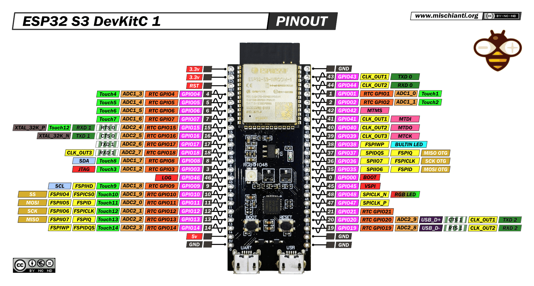
Click the image for the full high-resolution pinout and specs page at mischianti.org.
- CPU: Xtensa dual-core 32-bit LX7, up to 240 MHz
- GPIOs: ~45 usable
- ADCs: 2× 12-bit, multi-channel
- DACs: none (external MCP4922 dual 12-bit SPI DAC on the interface PCB)
- USB: native USB-OTG + USB-Serial-JTAG
- Wireless: Wi-Fi 4 + BLE 5
- Communication Interfaces: SPI, I²C, UART, CAN (TWAI), I²S
Dev-board mechanical reference (ESP32-S3-DevKitC-1)
The medulla PCB hosts the ESP32-S3 module via a stock ESP32-S3-DevKitC-1 dev board (or a pin-compatible clone such as the YD-ESP32-S3 / "44 pines tipo C"). The medulla footprint must match this:
| Quantity | Value |
|---|---|
| Pin pitch (within a row) | 2.54 mm (0.1 ″) |
| Pins per row | 22 (44 total — 2 rows of female sockets) |
| Row centerline ↔ row centerline | 22.86 mm (0.9 ″) |
| PCB outer width | 25.40 mm (= 22.86 + 2 × 1.27 mm edge offset) |
| USB-C protrusion past board edge | ~8.00 mm |
The row spacing is 22.86 mm (0.9 ″), NOT 25.40 mm. Pin centerlines are inset 1.27 mm from each PCB edge. This is confirmed by physical caliper measurement on an official Espressif board (2026-05-02). The Espressif DXF_…_V1.1_20220429.pdf mechanical drawing has ambiguous 1.27 mm callouts that can be read as either antenna keepout or pin-row offset, so trust the physical measurement, not any single drawing. Local mirrors of the Espressif drawing, schematic, and the ground-truth measurement photo are kept in the dv vault at dv/kart/kart-medulla/resources/esp32-s3-devkitc-1/.
ESP32-S3 Pin Assignment
The full 44-row pin table is not repeated here. It lives with the schematic, in
projects/kart-medulla/docs/pinout-esp32-s3.md
(dv-hardware), because a pin map is only correct relative to a schematic revision and the two have
to change in one commit. This page carries what you need with the board in front of you: which
pins do something other than their name, and what has been physically modified.
A hand-maintained copy of that table used to sit here. It drifted — on 2026-07-30 someone reconciled it row by row and left a note that two rows were deliberately ahead of dv-hardware; one day later dv-hardware caught up and the note became wrong. That is why there is now one table, not two.
For the per-pin capability reference (which GPIOs can do ADC, which are strap pins) see
lib/esp32-s3-pin-capabilities.md.
Pin numbers 1–44 follow a chip-style counter-clockwise convention: pin 1 is the bottom-right contact (USB-C at the top, component side facing you), pins 1–22 climb the right edge, pins 23–44 descend the left edge. Use these numbers when probing or talking about a contact — they are not the schematic-symbol pin numbers. The medulla's left header is dual-row (44 pads, 22 unique nets — each row is shorted between its two pads for daughterboard pass-through).
What the assembled board actually does
Board 84d6dd0 (the gerber-export commit, written on the board itself). Deviations from the pin
table only — everything not listed does what the table says.
| Pin | GPIO | Terminal | Name on the schematic | What it actually does |
|---|---|---|---|---|
| 19 | 1 | CN5.2 | PRESSURE_3 |
Reads the steering-angle sensor's PWM |
| 35 | 3 | CN8.2 | BUZZER |
Drives the EBS compressor MOSFET gate |
Both are permanent, and neither displaced anything: no pressure-3 sensor is fitted, and the kart
carries no buzzer or ASSI at all (those are formula-vehicle parts — settled 2026-07-18). The same two
rows, plus the planned throttle-PWM pin, are listed in the "As-built pin use" section of the
dv-hardware pinout file; physical modifications are tracked in that board's rework list in
projects/kart-medulla/README.md.
Two repurposed terminals on the current board
Detail for the two rows in the table above — what to do with a probe and a soldering iron. The firmware header km_gpio.h carries both (PIN_STEER_PWM_IN = GPIO 1, documented there as the MT6701's ~994 Hz PWM angle frame; PIN_CMD_COMPRESSOR = GPIO 3). The authoritative map is the schematic, with .agents/esp32s3-pinmap.md as its firmware-side copy.
- CN5.2 / GPIO 1 — steering-angle PWM (was
PRESSURE_3). The Pressure-3 ADC channel is retired; the terminal now reads the steering-angle sensor's single-wire PWM output — the wheel angle is encoded in the PWM duty cycle — decoded on the ESP32-S3 with the MCPWM capture peripheral (edge timing), not read as an analog voltage. Board rework: remove R10 only (the pulldown to GND), keeping R8 + R9. The net isCN5.2 —[R8 10k]— node —[R9 10k]— GPIO 1 —[R10 10k]— GND, so R10 is the only shunt to ground and R8 + R9 stay in place as a 20 kΩ series into the pin — too high-impedance for the ADC, which is why this pin reads digital PWM (MCPWM capture), not analog. This is the live path as of 2026-07-31: the MT6701 is mounted and validated working on the kart, reading over PWM — it replaced the AS5600/I²C arrangement rather than waiting as a later cleanup. See Angle Sensor and Wiring. - CN8.2 / GPIO 3 — EBS compressor PWM (was
BUZZER). The old buzzer output now drives the EBS air-compressor MOSFET gate (netCMD_COMPRESSOR_PWM); the buzzer was dropped. An external 100 kΩ gate pulldown holds the FET off through boot.
CMD_ACC and CMD_BRAKE go through the external SPI DAC
The classic ESP32 exposed CMD_ACC on a dedicated DAC pin. On the S3 there is no native DAC — both CMD_ACC and CMD_BRAKE are generated by the MCP4922 (dual 12-bit SPI DAC, see hardware decisions below) and ride the existing SPI bus (CS = GPIO 14). Channel A → CMD_ACC (0–5 V direct), Channel B → CMD_BRAKE → ×2 op-amp → 0–10 V for the Festo proportional brake valve.
GPIO restrictions (ESP32-S3)
Strap/boot pins on the S3 — notably GPIO 0, 3, 45, 46 — must be left at safe levels at reset; the table notes mark which assignments are constrained by this. On WROOM-1 modules some of GPIO 26–32 are tied to the SPI flash internally (always reserved). GPIO 33–37 are consumed by the octal PSRAM on the fitted module — see below.
Module fitted: ESP32-S3-WROOM-1-N16R8 — GPIO 33–37 are permanently unavailable
The module on the board is an ESP32-S3-WROOM-1-N16R8 (16 MB flash, 8 MB octal PSRAM). Confirmed on the hardware: esptool reports ESP32-S3 (QFN56) revision v0.2 with Embedded PSRAM 8MB (AP_3v3), and the firmware repo records the same module in AGENTS.md and .agents/esp32s3-pinmap.md.
GPIO 33–37 must never be assigned. On R8 modules the octal PSRAM die is hard-wired to those pins (the SPI0/1 extension pins) inside the module package, and Espressif's ESP32-S3-WROOM-1 datasheet marks them as not available. This is physical, not a firmware setting: disabling PSRAM in sdkconfig does not reclaim them, because the die stays electrically attached to the traces, and driving them externally risks bus contention during boot.
The pinout above already respects this — GPIO 33, 35, 36, and 37 are all HOLD with no signal routed, and CMD_REVERSE lives on the U25 PCF8574 expander (port P0) rather than on GPIO 36. MOTOR_HALL_1 was moved off GPIO 37 to GPIO 16 for the same reason. So the fitted R8 module costs the design nothing today; the constraint only bites if a future revision needs those five pins back.
Substituting a quad-PSRAM module is safe in the other direction. An N16R2 (16 MB flash, 2 MB quad PSRAM) or N8R2 (8 MB flash, 2 MB quad PSRAM) is a drop-in that frees GPIO 33–37 rather than consuming them, with no pinout change. Going the other way — assigning any of GPIO 33–37 and then fitting an R8 — is what breaks.
Historical note: N8R2 was the specified part from 2026-04-23 until 2026-07-30, and these docs previously carried a "do not buy R8" rule. An N16R8 was fitted instead, the pinout turned out to be R8-safe, and the rule was retired rather than the module swapped. Background in the dv vault, kart/kart-medulla/history.md (2026-04-23, 2026-04-29).
Kart Medulla Interface PCB
Interface PCB hosting the ESP32-S3 module, signal conditioning, the SPI DAC, the manual/autonomous analog mux, and outside-world connectors. Design lineage (EasyEDA .epro project files) lives in the Drive folder formula_24-25-26/dv/kart/kart-medulla/project-backups/.
Hardware Decisions
- Shutdown circuit (SDC): a single ESP32 GPIO —
SDC_NOT_EMERGENCYon GPIO 18 (Pin 33) — drives the gate of Q3 (IRLZ44N) through R22 (100 Ω). When HIGH, Q3 conducts and pulls the kart'sSDC_IN_LOW_SIDEto GND, completing the SDC return path → no emergency. When LOW, Q3 is off and the chain breaks → emergency. R23 (100 kΩ) gate-pulldown forces Q3 OFF (= emergency) at boot until firmware actively drives HIGH. The signal name reflects the intent the ESP32 asserts, not the chain's electrical state. There is no separateSDC_STATreadback in this rev — the ESP32 trusts its own command. (The previous design used a relay + a status pin on GPIO 38/39; replaced 2026-05-08 with the MOSFET-only scheme so the gate driver sits next to Q3 on the PCB layout.) - Analog command outputs (
CMD_ACC,CMD_BRAKE): external MCP4922-E/SL — dual 12-bit SPI DAC. On the existing SPI bus (CS = GPIO 14). VREF tied to the 5 V rail through a 100 Ω + 10 µF RC filter to attenuate ~150 kHz switching ripple from the upstream XW-1224 buck. Channel A →CMD_ACC0–5 V direct; Channel B →CMD_BRAKE→ ×2 op-amp → 0–10 V for the Festo proportional brake valve. Decision history: 2026-04-13 (initial choice was MCP4728 I²C) → 2026-04-17 (switched to MCP4922 SPI because we already had MCP4922 chips on hand and SPI is cleaner for an analog-command bus shared with no other slow devices). - Manual/autonomous signal mux (decision 2026-05-01, refined 2026-05-02 / 03 / 08): one MAX4660EUA+T SPDT analog switch (U14) on the PCB muxes the throttle signal between the manual source and the ESP32 DAC output. Brake is NOT muxed — manual mode does not need brake control routed through the ESP32, so the brake DAC output goes directly to the brake valve driver with no switch (decision 2026-05-08). Reverse is NOT muxed via MAX4660 nor via a direct ESP32 GPIO — it is driven by U25 PCF8574T port P0 (I²C GPIO expander) in parallel with the manual reverse button (wired-OR via the motor controller's existing pull-up; the PCF8574's quasi-bidirectional outputs are natively open-drain). This frees GPIO 36, which the fitted N16R8's octal PSRAM consumes (decision 2026-05-03). The MAX4660's SELECT pin is driven by
SELECT_THROTTLEon GPIO 15 with a 10 kΩ pulldown to GND, so the hardware default is manual passthrough whenever the ESP32 is crashed, hung, resetting, or unbooted. Steering is NOT muxed — the ESP32 always drives the Cytron H-bridge directly; in manual mode firmware sets PWM = 0. This means steering has no hardware safe state, unlike throttle and the compressor.CMD_STEER_PWMcarries no pull resistor, so it is undriven whenever the ESP32 is unbooted, resetting, crashed or removed — the entire bootloader window of every flash — while the Cytron stays powered from the 48 V pack. On 2026-08-08 the steering swung to full lock during a reflash and broke teeth off the steering gears. Until a pulldown is fitted (dv-hardwareprojects/kart-medulla/requirements.mdREQ-08), de-power the Cytron or unplug the steering motor before flashing. - Cytron H-bridge (steering driver) power (decision 2026-05-01): fed permanently from the 48 V traction pack — not from the 12 V rail, and NOT switched through the manual/autonomous mode switch. The MD25HV takes 7–58 V, so the pack is within spec. Permanent is the point: the Cytron's inrush capacitors were browning out the Orin every time the kart was switched into autonomous. The PCB only routes signals (
CMD_STEER_PWM,CMD_STEER_DIR) to the Cytron, not power. - REVERSE-signal driver to the kart electronics box —
Q4, a BSS123 (decision 2026-04-26, done): the driver is a BSS123 N-channel logic-level MOSFET (SOT-23), designator Q4, and it is fitted on the manufactured board. It replaced a PC357N1J000F optocoupler because medulla GND and box GND are bonded through several paths anyway (USB ↔ Orin, signals ↔ Cytron, motor return ↔ battery), so the opto's isolation was moot — the MOSFET is cheaper, smaller, faster, and doesn't age. The optocoupler was never placed on a schematic sheet; it exists only as an unused library entry in the EasyEDA source. Drives the box's REVERSE wire (5 V via ~60 kΩ internal pull-up; pull to 0 V to engage reverse). Note: older text called this partU12. There is no U12 on the board — the reference designators in the netlist areU1, U02, U5, U13, U14, U19, U23, U24, U25, and dv-hardware's pinout doc separately flags U12 as redundant. UseQ4. - Pressure sensor inputs (3× Festo, 24 V): voltage divider + input clamp / TVS protection on each channel to bring the signal into the S3's ADC range (≤ 3.3 V).
- Hydraulic pressure sensor inputs (2×): routed to ADC1_CH9 (GPIO 10) and ADC1_CH1 (GPIO 2).
- Hall sensor inputs (3× 5 V): dedicated level translator (NOT the optocoupler) to 3.3 V before the GPIO pins.
- Orin link: UART0 over the DevKitC-1's on-board WCH CH343 bridge (the
COMUSB-C port), 115200 baud, appearing on the Orin as/dev/ttyACM0. The PCB adds no bridge chip of its own. GPIO 19/20 (D∓) go to the module's native USB port, which is wired but unused — switching the Orin onto it would move the serial console too, so it is not a drop-in change. - Power architecture: kart 12 V → external XW-1224 buck → 5 V kart-wide rail → medulla 5 V (H1.21) → ESP32-S3 module LDO → 3.3 V. The medulla can alternatively be powered from an on-board LM2596SX-ADJ buck (qty 8 in stock) if the kart-wide 5 V rail is unavailable. MCP4922 VDD and MAX4660 Vcc both run from the same 5 V rail.
Connector Pinout (Outside World)
The fabricated ESP32-S3 interface PCB brings every outside-world signal to ten 3-pin green push-in headers, CN1–CN10 (per the board's F.Silkscreen layer).
What is on each terminal: Connector Pinout (CN1–CN10). That page carries the per-connector assignment table, the silkscreen block, the physical pin-order rules, and the two naming traps (BUZZ on CN8.2 is not a buzzer; EXP_P2 is CN3.2). It is generated from the schematic-side file in dv-hardware — see the banner at the top of it.
Which wire runs where: the whole-kart wire list. One row per net; search the Connected pins column for medulla.CNx.y. Which GPIO a terminal reaches: projects/kart-medulla/docs/pinout-esp32-s3.md in dv-hardware. Signal names follow the Net Name Nomenclature convention.
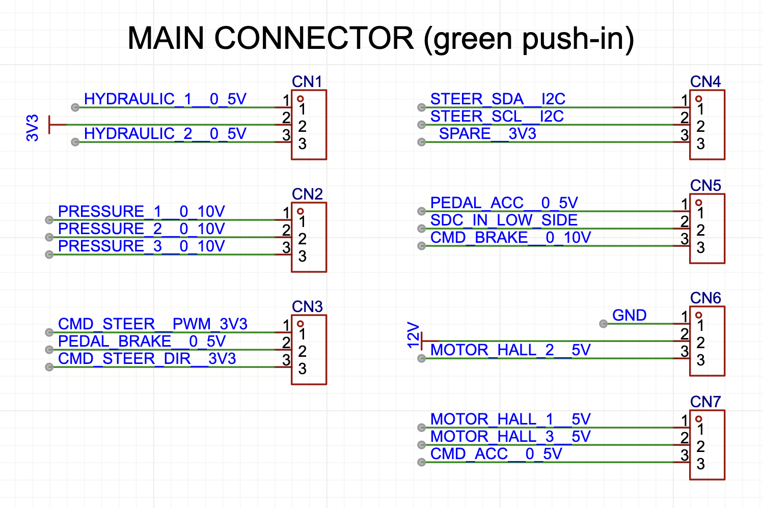
Terminal notes that aren't obvious from the wire list:
- CN1–CN10 are 3-pin. Supplies sit on CN1 (+3V3 / +12V / GND), CN2.3 (+5V), CN6.3 (+3V3), CN9.3 and CN10.3 (GND).
- EXP_P1..P4 (CN3.1–3, CN5.3) are port pins of the on-board U25 PCF8574 I²C GPIO expander (address 0x20) brought out to terminals — for example
CMD_REVERSElives on PCF8574 P0, not on a native GPIO. - CN4.3 REV is the reverse-command wire to the kart electronics box (driven by
Q4, the BSS123; 5 V idle via the box's internal pull-up, pulled to 0 V to engage reverse). CN4 carries no 3V3/GND. - CN5.2 (ex-PRES3) and CN8.2 (ex-BUZZ) are the two repurposed terminals — steering-angle PWM and EBS-compressor PWM respectively (see the callout under the pin table).
- CN8.1 SDC is
SDC_IN_LOW_SIDE, the Q3 drain that closes the kart shutdown chain's return path. The ESP32 side of that MOSFET (SDC_NOT_EMERGENCY, GPIO 18) is internal and deliberately not on any terminal. - CN10 analog commands come from the MCP4922 SPI DAC (the S3 has no native DAC).
Physical pin order runs opposite on the two sides
Pin 1 is at the top on CN1–CN5 (right side, footprint rotation −90°) and at the bottom on CN6–CN10 (left side, +90°) — verified against kart-medulla.kicad_pcb on 2026-07-10, superseding an earlier "1/2/3 top to bottom" reading that only held on the right. Because the CNs themselves advance bottom→top on the right and top→bottom on the left, pin numbering runs counter to connector numbering on both sides. Details and the staggered-footprint consequence are on the Connector Pinout page.